
usb e kits presents
clap switch V2
|
|
|
functionality
A very cool clap switch kit!
Simply clap your hands twice to energise or dienergize electrical or electronic devices.
The board output can handle up to 6 amps.
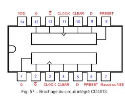
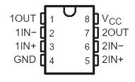
The kit is based on a dual amplifier (LM358) and general purpose flip-flop 4013.
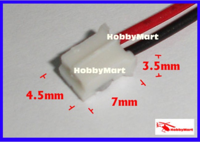
Mic converts the sound signals from your claps into small electrical signals.
The first opamp of the lm358 amplify these small signals.
Then the amplificated pass through a peak detector circuit.
The second opamp opperates as a comparator.
With the potensiometer in series with resistor R6 provides us the required reference voltage (0-3.8 volt).
This is our sensitivity control.
The output of the comparator lights up the blue led (that indicates to us the clap)
and triggers the cd4017 dual flip-flop.The first flip-flop change its output.
Because of the three state arrangement of the flip-flop ,
one more clap is needed to change the output state of the second flip-flop.
Second clap sets the flip-flop output to high and this forward biases a npn transistor (2N3904).
The transistor drives a Relay and then you can get both the N.O. and the N.C output contacts
through a 3 pin terminal block.The maximum load should be less than 6 amps continously.
The connected device to the relay switches on.
Same procedure applies for the opposite.
When you clap your hands twice, relay closes and turns off the device connected to it.
You can adjust the sensitivity of the circuit via the 50k trimmer.
When you first power up turn the trimmer until blue led turns on.
This is the start point.
The trimmer has 25 turns until the lowest sensitivity level.
You should adjust the trimmer till the room noise does not affect the switch operation.
Simply clap your hands twice to energise or dienergize electrical or electronic devices.
The board output can handle up to 6 amps.
The kit is based on a dual amplifier (LM358) and general purpose flip-flop 4013.
Mic converts the sound signals from your claps into small electrical signals.
The first opamp of the lm358 amplify these small signals.
Then the amplificated pass through a peak detector circuit.
The second opamp opperates as a comparator.
With the potensiometer in series with resistor R6 provides us the required reference voltage (0-3.8 volt).
This is our sensitivity control.
The output of the comparator lights up the blue led (that indicates to us the clap)
and triggers the cd4017 dual flip-flop.The first flip-flop change its output.
Because of the three state arrangement of the flip-flop ,
one more clap is needed to change the output state of the second flip-flop.
Second clap sets the flip-flop output to high and this forward biases a npn transistor (2N3904).
The transistor drives a Relay and then you can get both the N.O. and the N.C output contacts
through a 3 pin terminal block.The maximum load should be less than 6 amps continously.
The connected device to the relay switches on.
Same procedure applies for the opposite.
When you clap your hands twice, relay closes and turns off the device connected to it.
You can adjust the sensitivity of the circuit via the 50k trimmer.
When you first power up turn the trimmer until blue led turns on.
This is the start point.
The trimmer has 25 turns until the lowest sensitivity level.
You should adjust the trimmer till the room noise does not affect the switch operation.
After your feedback from the first version we made some improvements
please leave your feedback for the kit or your suggestions for more improvements in the future
|

|
V2 release improvements
1) Reverse polarity protection
2) Redusing the noise in the nets with better pcb wiring and by adding capacitors above the chips.
3) Bigger pads for easier constructions
4) Better placing of the components for easier constructions
5) The on/off switch now is extended from the pcb so you can mount it in your project box
6) Output contacts now can handle about 6 amps.
7) The trimmer are now extended from the pcb board so you can mount them in your project box.
8) Bigger heat sink power plates for better heat consumption.
9) A blue led indicates the clap and helps you to check if the sensitivity you want is ok.
10)Start point of highest sensitivity level with the blue led
11)Better amplification of the electrical signals of the mic with opamp.
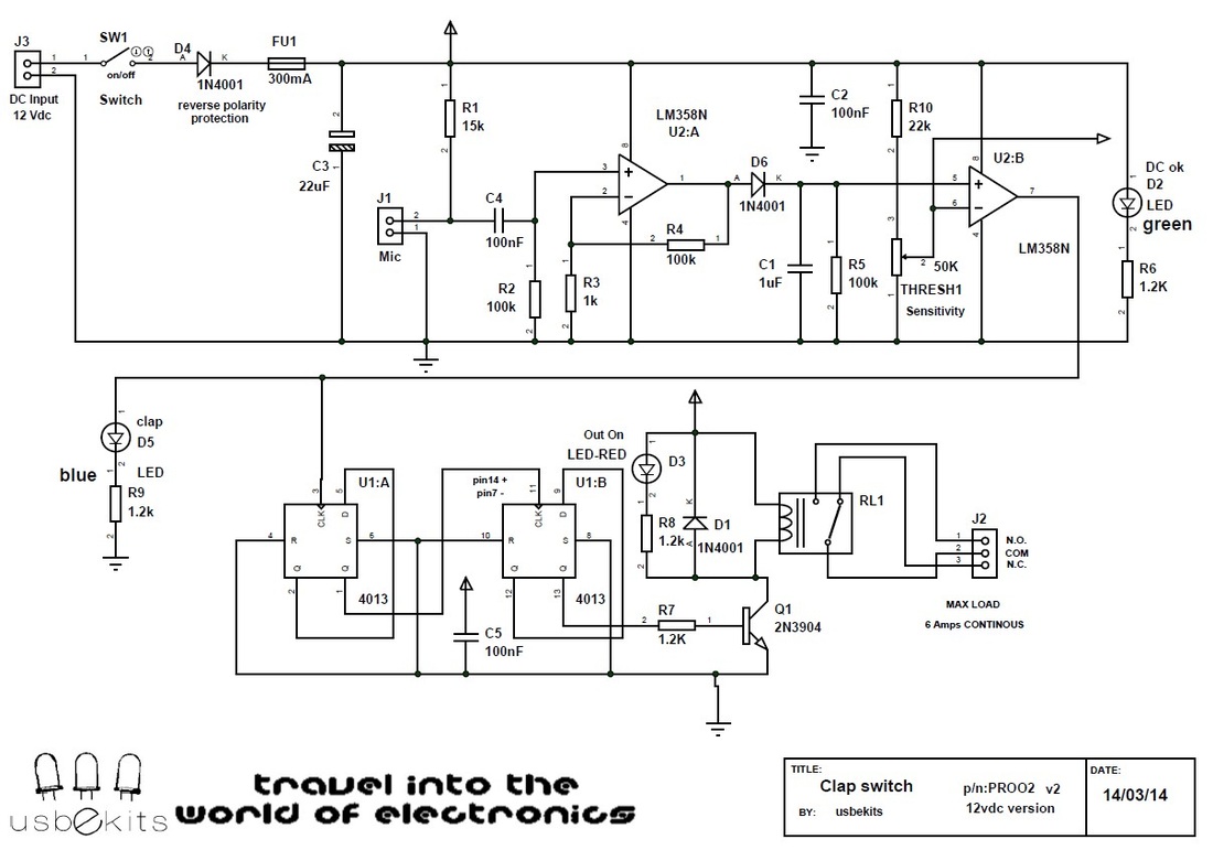
the circuit schematic
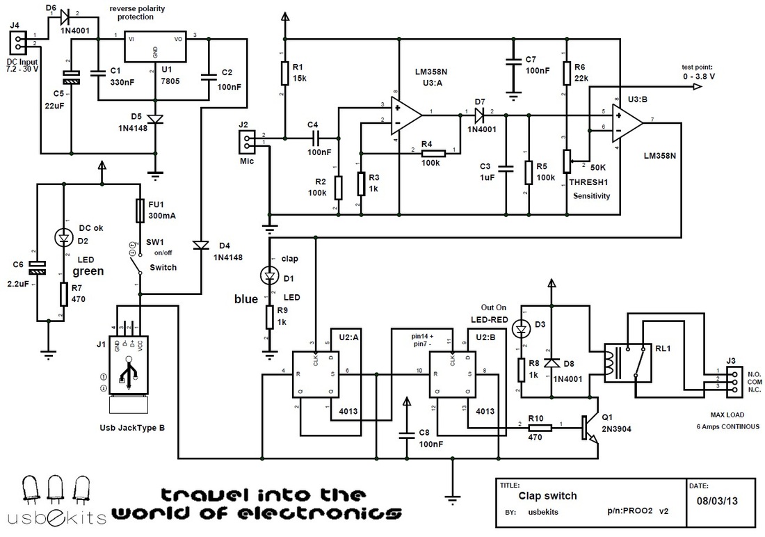
Clap switch schematic
part list
Reference Type Value
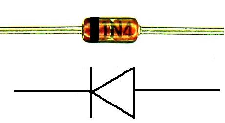
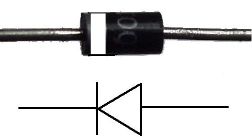
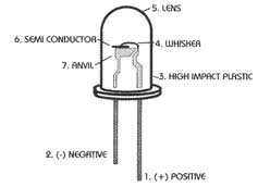
C1 Ceramic Capacitor 330nF C2 Ceramic Capacitor 100nF C3 Ceramic Capacitor 1uF C4 Ceramic Capacitor 100nF C5 Electrolytic Capacitor 22uF C6 Electrolytic Capacitor 2.2uF C7 Electrolytic Capacitor 2.2uF C8 Smd 0603 Capacitor 100n D1 3mm Diffused Led Blue D2 3mm Diffused Led Green D3 3mm Diffused Led Red D4 High speed Diode 1N4148 D5 High speed Diode 1N4148 D6 rectifier Diode 1N4001 D7 rectifier Diode 1N4001 D8 rectifier Diode 1N4001 FU1 Fuse Glass 20mm 300ma J1 Usb jack Type B J2 jst 2pin cable Mic input J3 Terminal Block 3 pin contacts output J4 Terminal Block 2 pin Dc input Q1 NPN Transistor 3904 R1 RESISTOR 15k R2 RESISTOR 100k R3 RESISTOR 1k R4 RESISTOR 100k R5 RESISTOR 100k R6 RESISTOR 22k R7 RESISTOR 470 R8 RESISTOR 1k R9 RESISTOR 1k R10 RESISTOR 470 RL1 Relay double contacts 5V coil RV1 jst 3pin cable 3296 Trimmer 50k SW1 jst 2 pin cable ON/OFF Switch U1 Voltage Regulator 7805 U2 Flip-Flop 4013 U3 dual opamp LM358 |
construction help guide
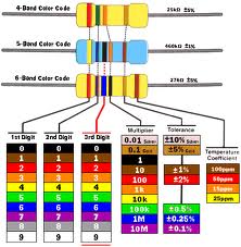
resistor color code definition
|


downloads
| clap_switch_v2_datasheet.pdf |
| clap_switch_proo1v2_merged.pdf |
A more friendly to use schematic for 12 vdc power supply
As I notice a lot of people get confused when they try to build their own schematic. The complexicity in the power input is one of the major problems for the usb power input.So i decide to design a more friendly schematic for those who want to use a 12 power supply only directly.So have a look at this:
Clap your hands twice
to switch on and off varius devices!

|
|