usbekits
  • HOME
  • ELECTRONICS
    • OUR KITS >
      • COLOR ORGAN external lights
      • 555 PWM CONTROLLER
      • CLAP SWITCH
      • DARK DETECTOR
      • RGB MOOD LAMP
      • COLOR ORGAN
      • LED VOLTMETER
      • DC TO DC CONVERTER
    • CALCULATORS & CONVERTERS
    • SOLDERING & PROTOTYPING
    • PICTORIALS
    • CIRCUITS AND TUTORIALS
    • DATASHEETS
  • 3D PRINT
    • CUSTOM LED MACHINE VISION
  • PROJECTS
    • 3 FLOOR ELEVATOR LOGO
    • 3 FLOOR ELEVATOR ARDUINO
    • ARDUINO I/O BOARD
    • VERTICAL AXIS WIND TURBINE
    • MOBILE SOLAR PANEL
  • BLOG / NEWS
  • CONTACT US
  • ORAMA
  • LINKS

omron g3mb-202p solid state relay datasheet

3/18/2014

0 Comments

 
Picture
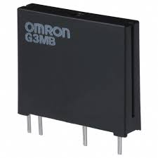
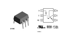
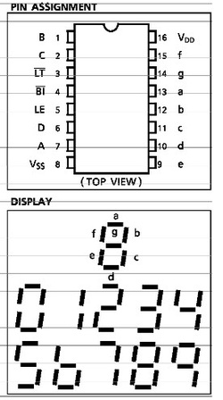
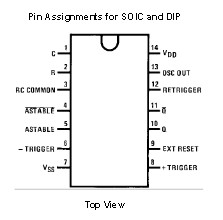
Low cost Subminiature PCB mounting 2 amp Single in-line package (SIP) SSR
• Bottom is approximately 3 times smaller than G3M.
• Low cost “SIP” package switches up to 2A loads.
• Built in Snubber circuit and input resistor as option.
• Two footprints available for design flexibility.
• The G3MB-202PEG-4-DC20MA crosses directly to the Motorola M0C2A-60 series power triac
http://www.sainsonic.com/zen/albums/ebay/nichegeek/20-018-200/05577d01.pdf

0 Comments

New datasheet for clap switch kit

3/15/2014

0 Comments

 
Picture
We added the updated datasheet of the clap switch kit

check it out here<------------

0 Comments

TL431

12/4/2013

0 Comments

 
Picture
The TL431/TL431A are three-terminal adjustable regulatorseries with a guaranteed thermal stability over applicabletemperature ranges. The output voltage may be set to anyvalue between VREF (approximately 2.5 volts) and 36 voltswith two external resistors.
datasheet here<--------------


0 Comments

Ina 128,129  instrumantation amplifiers

11/25/2013

0 Comments

 
Picture
The INA128 and INA129 are low power, generalpurpose instrumentation amplifiers offering excellentaccuracy. The versatile 3-op amp design and small sizemake them ideal for a wide range of applications.Current-feedback input circuitry provides widebandwidth even at high gain (200kHz at G = 100).
datasheet here<-------

0 Comments

cd4041ub quad true/complement buffer datasheet

9/10/2013

0 Comments

 
Picturecd4041ub quad true/complement buffer
The CD4041UB/CD4041UBC is a quad true/complementbuffer consisting of N- and P-channel enhancement modetransistors having low-channel resistance and high current(sourcing and sinking) capability. The CD4041 is intendedfor use as a buffer, line driver, or CMOS-to-TTL driver.All inputs are protected from static discharge by diodeclamps to VDDand VSS.

datasheet here<----


0 Comments

4n25,4n26,4n27,4n28 optocouplers datasheet

9/10/2013

0 Comments

 
Picture4n25,4n26,4n27,4n28 optocouplers
The 4N25 family is an industry standard single channelphototransistor coupler. This family includes the 4N25,4N26, 4N27, 4N28. Each optocoupler consists of galliumarsenide infrared LED and a silicon NPN phototransistor.

datasheet here<---

0 Comments

lm741 operational amplifier

9/10/2013

0 Comments

 
Picturelm741 operational amplifier
general purpose operational amplifier

datasheet here<--------

0 Comments

74ls374 octal d-type flip-flop datasheet

9/10/2013

1 Comment

 
Picture74ls374 octal d-type flip-flop
These 8-bit registers feature totem-pole 3-STATE outputsdesigned specifically for driving highly-capacitive or rela-tively low-impedance loads. The high-impedance state andincreased high-logic level drive provide these registers withthe capability of being connected directly to and driving thebus lines in a bus-organized system without need for inter-face or pull-up components. They are particularly attractivefor implementing buffer registers, I/O ports, bidirectional busdrivers, and working registers

datasheet here<-----


1 Comment

4526 bcd to 7 segment datasheet

9/10/2013

0 Comments

 
Picture4526 bcd to 7 segment
bcd to 7 segment driver

datasheet here<-------

0 Comments

4047 monostable multivibrator datasheet

9/10/2013

0 Comments

 
Picture4047 monostable multivibrator
The CD4047B is capable of operating in either themonostable or astable mode. It requires an external capac-itor (between pins 1 and 3) and an external resistor(between pins 2 and 3) to determine the output pulse widthin the monostable mode, and the output frequency in theastable mode.Astable operation is enabled by a high level on the astableinput or low level on the astable input. The output fre-quency (at 50% duty cycle) at Q and Q outputs is deter-mined by the timing components. A frequency twice that ofQ is available at the Oscillator Output; a 50% duty cycle isnot guaranteed.Monostable operation is obtained when the device is trig-gered by LOW-to-HIGH transition at + trigger input orHIGH-to-LOW transition at − trigger input. The device canbe retriggered by applying a simultaneous LOW-to-HIGHtransition to both the + trigger and retrigger inputs.A high level on Reset input resets the outputs Q to LOW, Qto HIGH.

datasheet here<---------

0 Comments
<<Previous

    usbekits

    Read our latest Posts!Share your thoughts!Edit your comments here!
    This blog started at 20/10/12

    Archives

    May 2014
    March 2014
    December 2013
    November 2013
    October 2013
    September 2013
    July 2013
    June 2013
    April 2013
    March 2013
    February 2013
    January 2013
    December 2012
    November 2012
    October 2012

    Categories

    All
    Admin
    Circuits
    Datasheets
    Educate
    Electronic Parts
    Links
    Pictorials
    Site Updates

    RSS Feed

    Picture
Powered by Create your own unique website with customizable templates.