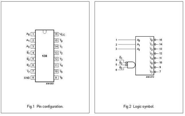
datasheet here<----------
![]() The 74AHC/AHCT138 are high-speed Si-gate CMOS devices and are pincompatible with low power Schottky TTL (LSTTL). They are specified incompliance with JEDEC standard No. 7A.The 74AHC/AHCT138 decoders accept three binary weighted address inputs(A0,A1and A2) and when enabled, provide 8 mutually exclusive active LOWoutputs (Y0toY7).The ‘138’ features three enable inputs: two active LOW (E1andE2) and oneactive HIGH (E3). Every output will be HIGH unlessE1andE2are LOW and E3is HIGH.This multiple enable function allows easy parallel expansion of the ‘138’ to a1-of-32 (5 to 32 lines) decoder with just four ‘138’ ICs and one inverter.The ‘138’ can be used as an eight output demultiplexer by using one of theactive LOW enable inputs as the data input and the remaining enable inputs asstrobes. Unused enable inputs must be permanently tied to their appropriateactive HIGH or LOW state.The ‘138’ is identical to the ‘238’ but has inverting outputs. datasheet here<----------
0 Comments
![]() The μA723 is a precision integrated-circuitvoltage regulator, featuring high ripple rejection,excellent input and load regulation, excellent temperature stability, and low standby current. The circuit consistsof a temperature-compensated reference-voltage amplifier, an error amplifier, a 150-mA output transistor, andan adjustable-output current limiter.The μA723 is designed for use in positive or negative power supplies as a series, shunt, switching, or floatingregulator. For output currents exceeding 150 mA, additional pass elements can be connected as shown inFigures 4 and 5.The μA723C is characterized for operation from 0°C to 70°C datasheet here<-------- ![]() The B Series logic gates are constructed with P and N channelenhancement mode devices in a single monolithic structure(Complementary MOS). Their primary use is where low powerdissipation and/or high noise immunity is desired. datasheet here<------ ![]() This device contains four independent gates each of which performs the logic NOR function datasheet here<--------- ![]() -MEDIUM-SPEED OPERATION. -FULLY STATIC OPERATION. -COMMON RESET. -BUFFERED INPUTS AND OUTPUTS. -QUIESCENT CURRENT SPECIFIED TO 20VFOR HCC DEVICE. -STANDARDIZED SYMMETRICAL OUTPUT.CHARACTERISTICS. -5V, 10V, AND 15V PARAMETRIC RATINGS. -INPUT CURRENT OF 100nA AT 18V AND25°C FOR HCC DEVICE. -100% TESTED FOR QUIESCENT CURRENT. -MEETS ALL REQUIREMENTS OF JEDEC TEN-TATIVE STANDARD No. 13A, ”STANDARDSPECIFICATIONS FOR DESCRIPTION OF ”B”SERIES CMOS DEVICES datasheet here<--------- ![]() The MC14069UB hex inverter is constructed with MOS P−channeland N−channel enhancement mode devices in a single monolithicstructure. These inverters find primary use where low powerdissipation and/or high noise immunity is desired. Each of the sixinverters is a single stage to minimize propagation delays. datasheet here<--------- ![]() This is an N-Channel enhancement mode silicon gate power field effect transistor designed for applications such as switching regulators, switching converters, motor drivers, relay drivers and drivers for high power bipolar switching transistors requiring high speed and low gate drive power. This type can be operated directly from integrated circuits datsheet here<----------- |
usbekitsRead our latest Posts!Share your thoughts!Edit your comments here! Archives
May 2014
Categories
All
|